EN

RF Attenuator Design Basics: T, Pi, and Key Performance Parameters
Fixed attenuators look simple: a few resistors that reduce a signal by a known number of decibels. In practice, rf attenuator design is a matching problem as much as a loss problem. A pad must deliver the intended attenuation while presenting the correct impedance to both sides of an RF path. If it does not, reflections can change the measured loss, disturb a source or load, and make a clean-looking calculation perform poorly at frequency.
For 50-ohm systems, T and Pi pads are two of the most useful starting points. They are passive, reciprocal resistor networks that can be designed for equal source and load impedances or adapted for impedance transformation. This article focuses on the equal-impedance case, then connects the circuit choice to frequency range, power handling, VSWR, and attenuation accuracy.
Start with the system requirement, not the resistor values
A disciplined rf attenuator design starts with five questions: What attenuation is required? What is the reference impedance? What frequency band must remain flat? What average and peak power can occur? And how much mismatch can the surrounding system tolerate? The desired attenuation alone is not a complete specification.
For example, a 10 dB pad in a 50-ohm test path should ideally look like 50 ohms at its input and 50 ohms at its output. That is why a properly designed pad can improve isolation between blocks even though it intentionally reduces signal level. The attenuation absorbs some reflected energy and helps each connected block see a more stable impedance.
At its simplest, calculate the voltage ratio as K = 10A/20, where A is attenuation in dB. Resistor formulas then follow from the requirement that both ports remain matched. Calculate first, select practical resistor values second, and verify the assembled network last.
T attenuator: a series-friendly topology
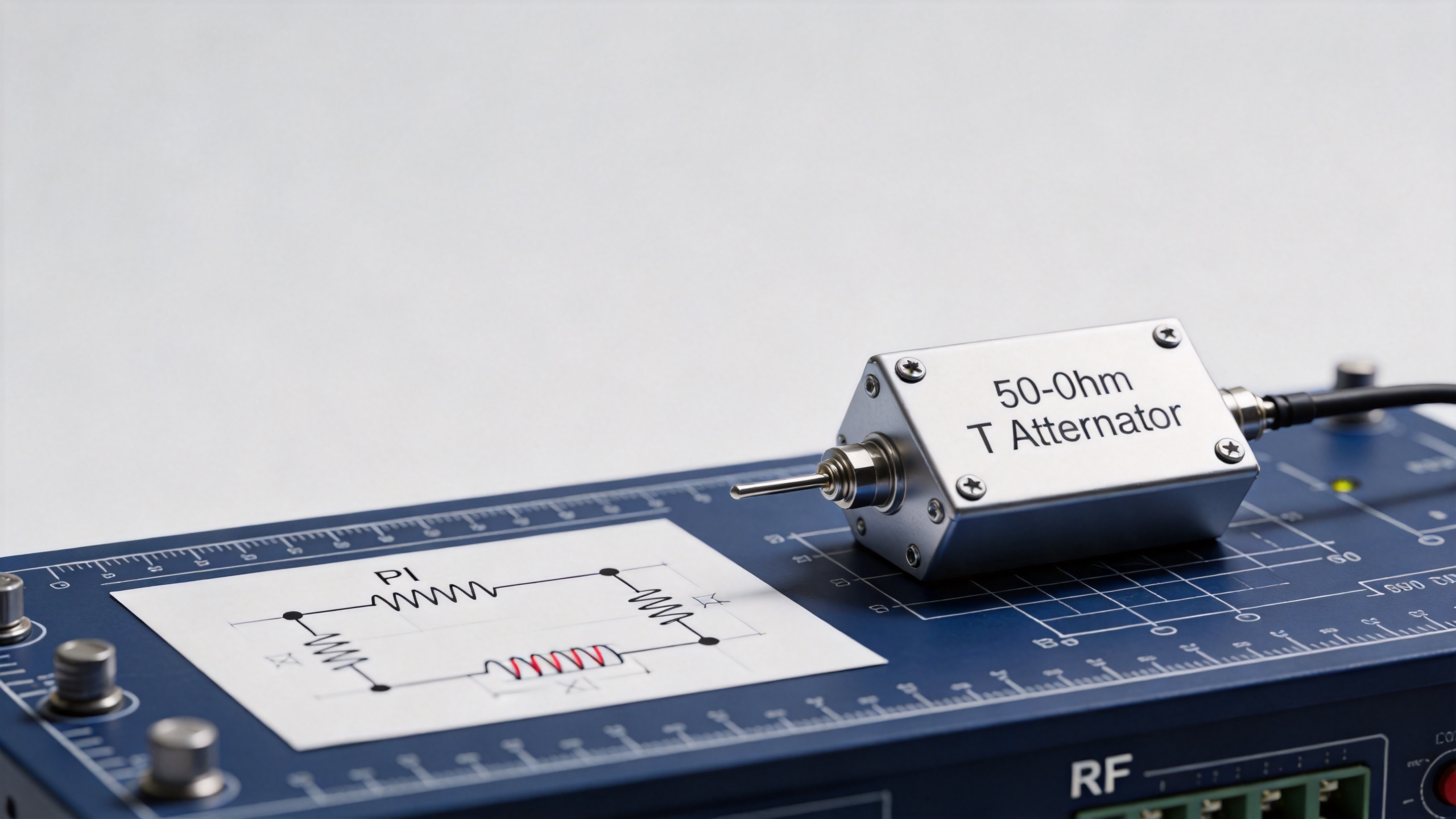
A symmetric T attenuator uses two series resistors with a shunt resistor between them. It is often easy to understand because the signal path visibly passes through two series arms. For equal reference impedances Z0, the standard ideal relationships are:
- Each series arm: Rseries = Z0(K − 1)/(K + 1)
- Center shunt arm: Rshunt = 2Z0K/(K2 − 1)
In a 50-ohm system, these equations provide an ideal resistor set before preferred-value rounding, tolerance analysis, and parasitic modeling. A T pad can be convenient where a series break already exists in the layout or where the center node can be grounded with a short, low-inductance connection.
The trade-off is physical. At higher frequencies, the series-resistor pads and the grounded center connection add parasitic inductance and capacitance. A layout that is electrically short at low frequency may no longer behave as a lumped network near the upper end of the band. The topology is still valid; the implementation must be verified with the actual resistor package, land pattern, and connector transition.
Pi attenuator: a shunt-friendly topology
A symmetric Pi attenuator uses two shunt resistors—one at each port—and a series resistor between them. It is electrically equivalent in purpose to a T pad for equal source and load impedances, but its geometry can fit a different board or coaxial layout. A Pi pad is often attractive when both ports have convenient ground access and the series element can be kept short between them.
Neither topology wins in every layout. Choose the network that preserves a continuous RF ground, keeps current-loop area small, and puts resistor parasitics where they do the least harm. That practical fit matters more than choosing T or Pi by habit.
| Decision factor | T pad | Pi pad |
|---|---|---|
| Physical pattern | Two series arms and one center shunt | One series arm and shunts at both ports |
| Useful layout condition | A natural series break with a short center ground | Strong ground access at both port nodes |
| Common design goal | Matched attenuation in a compact series path | Matched attenuation with port-side shunt control |
| What to verify | Series parasitics and center-via inductance | Shunt-ground quality and port discontinuities |
Key performance parameters that decide whether the pad works
Attenuation value and flatness
Nominal attenuation is the specified reduction at a reference condition. In a real rf attenuator design, the more useful question is how far the attenuation moves across the required band and temperature range. Resistor tolerance, frequency-dependent parasitics, connector transitions, and nearby metalwork can all change the result. For wideband work, request or measure attenuation versus frequency rather than relying on a single center-frequency number.
Frequency range
A resistor network has no sharp cutoff in the ideal circuit model, but its package and layout do. Keep interconnects short, avoid long ground returns, and model or measure the completed assembly with a vector network analyzer when the operating band makes parasitics meaningful. An attenuator rated far above the system band is not automatically a better purchase; extra margin should solve a real frequency or mismatch requirement.
VSWR and return loss
VSWR and return loss describe impedance match. Good matching matters because reflections alter both delivered power and measurement confidence. A pad can be inserted to improve isolation, but only if the pad itself maintains a suitable match over the operating band. Review input and output VSWR separately when the application is directional or when source and load conditions are not identical.
Power handling and resistor dissipation
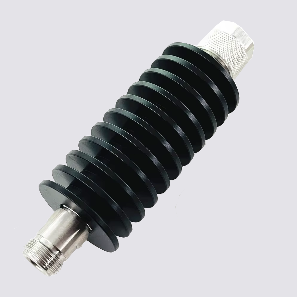
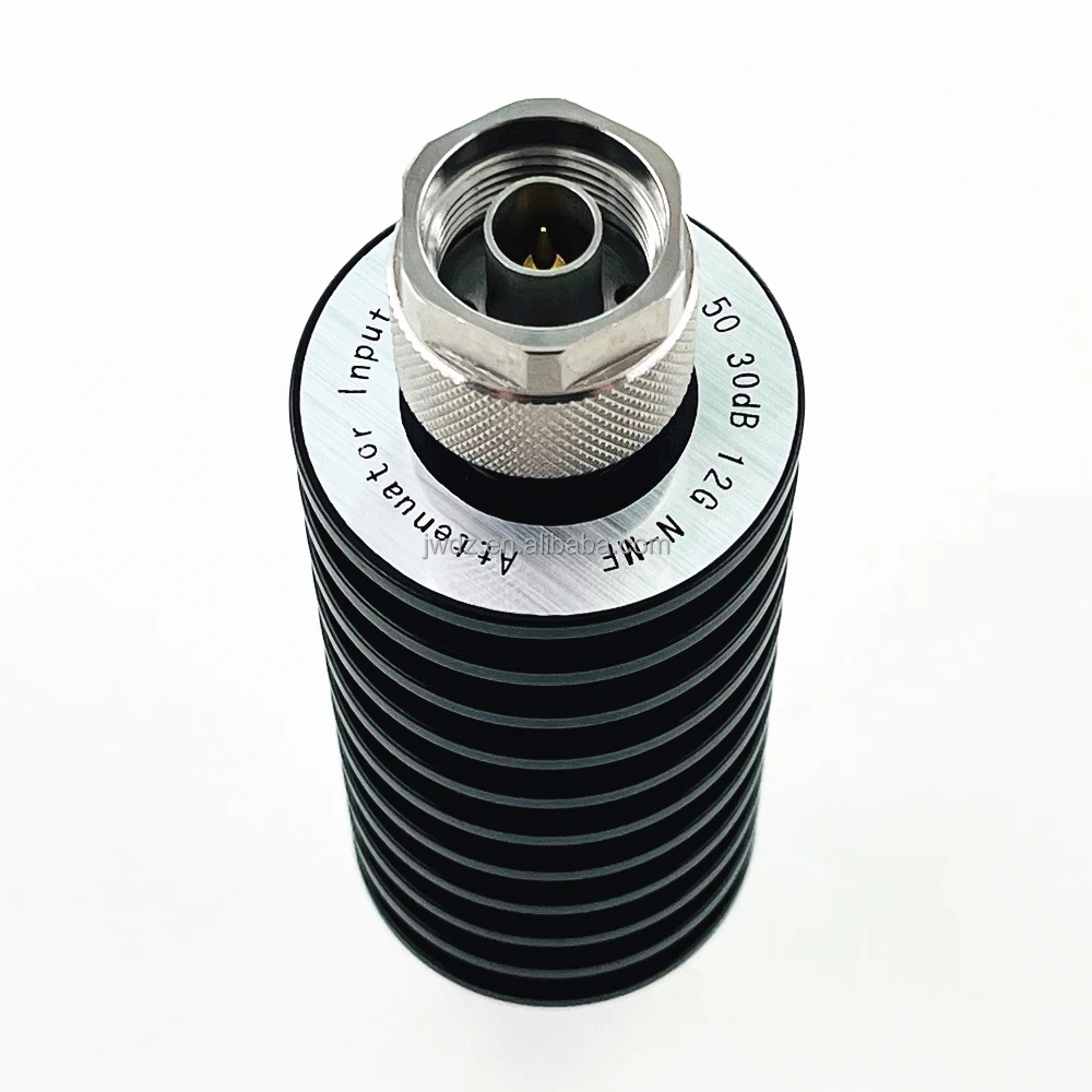
Total input power is not enough. The resistor that absorbs the largest share of energy may reach its temperature limit first, especially at high attenuation or with a mismatched load. Check average power, peak power, pulse conditions, heatsinking, and resistor derating. For higher-power coaxial applications, a catalog component may be preferable to a board-level pad because package construction, thermal path, and connector interface are part of the rating.
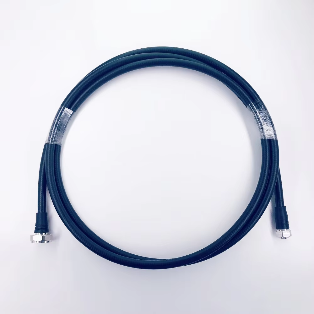
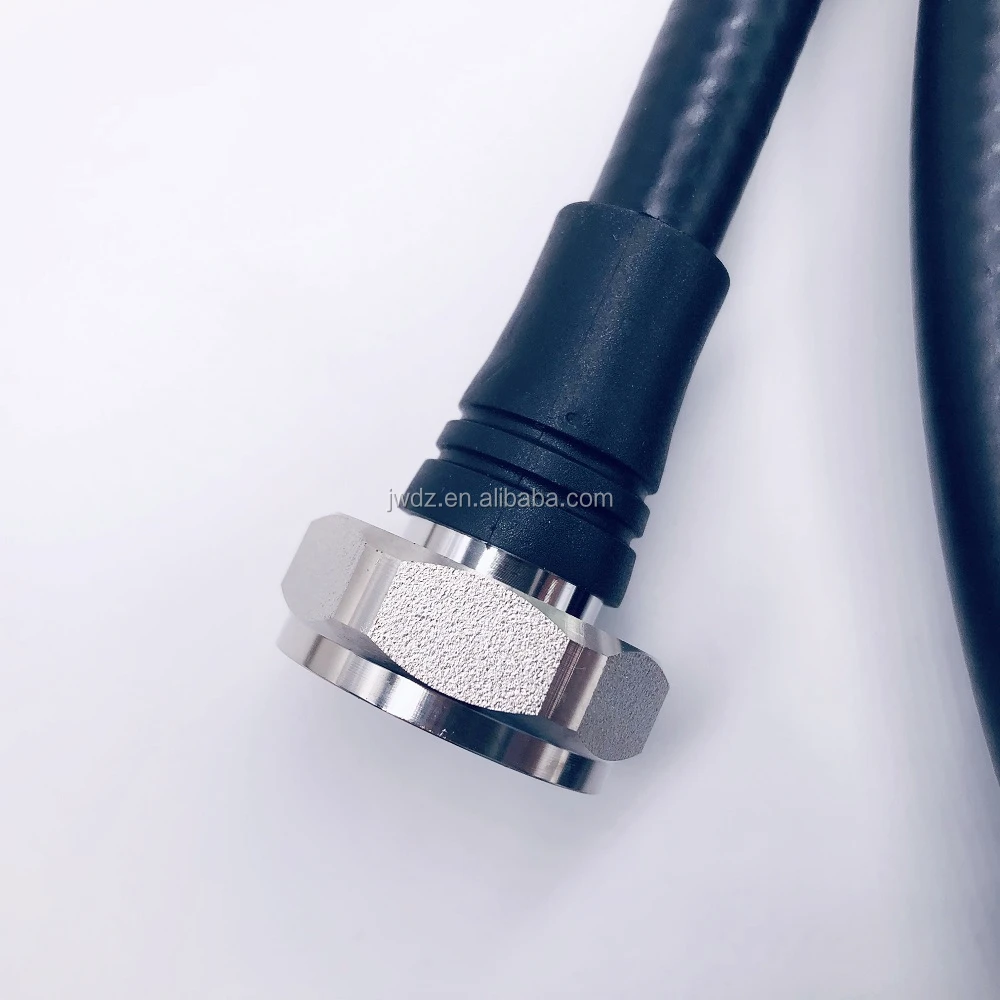
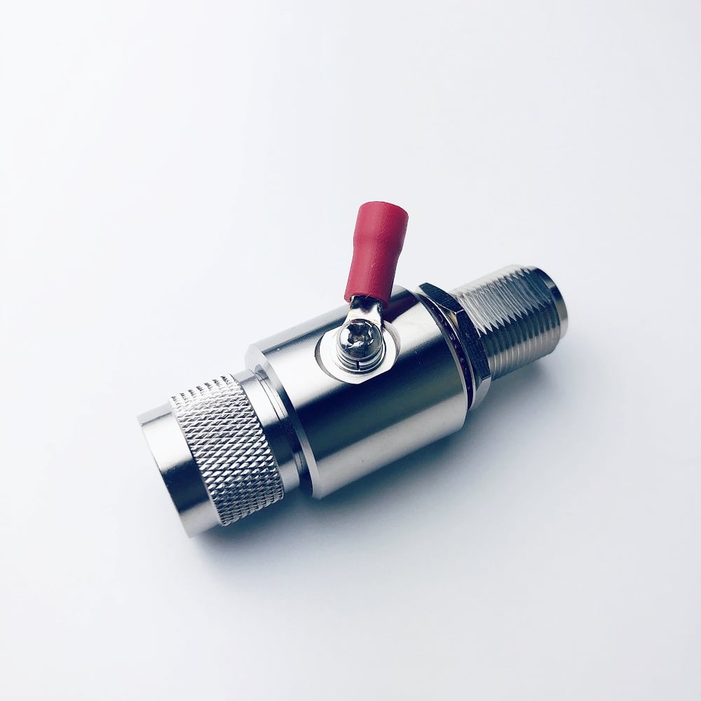
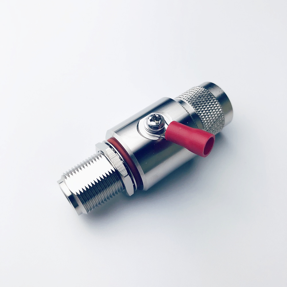
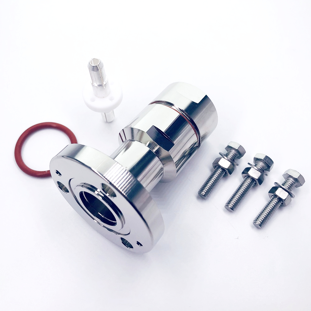
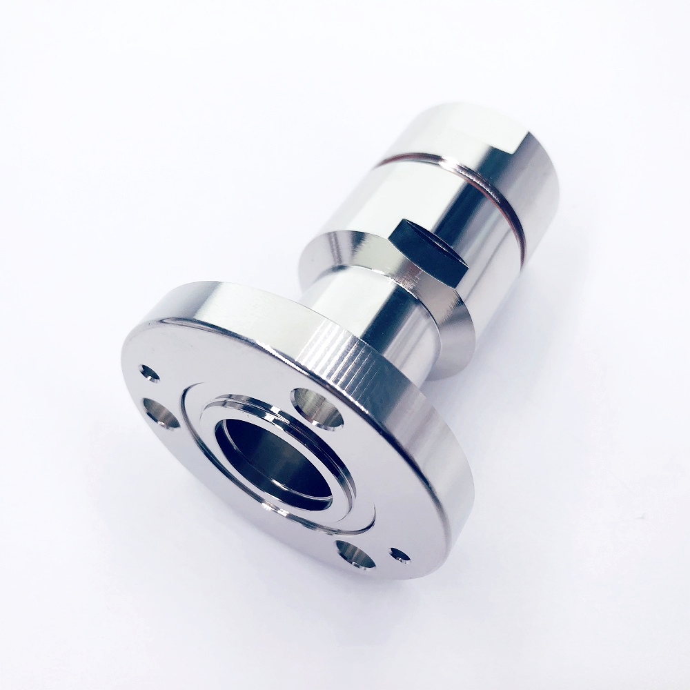
Where a packaged solution fits the required band and interface, a product such as this 100W 4.3/10 coaxial attenuator can be evaluated against the application specification. Confirm the published attenuation option, operating band, power conditions, and connector compatibility before selection.
A practical verification sequence
- Set attenuation, reference impedance, frequency band, and power conditions.
- Calculate ideal T or Pi values for the matched system.
- Select resistor values and packages with tolerance, voltage, and thermal margins.
- Lay out the network with a short RF path and low-inductance ground returns.
- Measure S-parameters across the full operating band, then check power behavior under the intended duty cycle.
One useful reminder: low insertion loss is not the objective of an attenuator. Controlled loss with repeatable impedance is. When the T or Pi topology, resistor technology, and mechanical implementation are all aligned with the system requirement, the resulting pad becomes a predictable RF building block rather than an uncertain source of reflections.
RF attenuator design checklist for common decisions
Use this short checklist when reviewing an rf attenuator design. It converts a resistor calculation into a component-selection decision.
Does the rf attenuator design match the system impedance?
An rf attenuator design for 50 ohms is not automatically correct for a 75-ohm path. Confirm source and load impedance before calculating a T pad or Pi pad. If they differ, use a matching-attenuator calculation rather than forcing an equal-impedance formula.
Is the rf attenuator design specified across the real band?
State the lowest and highest operating frequencies. A credible rf attenuator design includes attenuation tolerance and VSWR across that whole range, not only at one nominal frequency.
Can the rf attenuator design survive the real power duty cycle?
Review continuous, peak, pulse, and mismatch conditions. In a high-power rf attenuator design, resistor temperature rise and thermal spreading can be more limiting than the nominal dB value.
Has the rf attenuator design been measured after assembly?
Bench calculations establish a target; network-analyzer data validates the completed rf attenuator design. Measure S11, S22, and S21, then compare them with the original attenuation and match requirements.
For a purchasing review, record topology, nominal attenuation, impedance, frequency band, maximum power, connector type, and VSWR in the RFQ. That makes the rf attenuator design requirement testable across suppliers.
For a production release, specify the acceptance window for attenuation and return loss. A repeatable rf attenuator design is defined by measured limits, not by the schematic alone.
Frequently asked questions about rf attenuator design
Which topology should I choose for rf attenuator design?
Choose T or Pi based on the layout and grounding geometry. In rf attenuator design, both can create a matched fixed pad when their values and physical implementation are correct.
Why does VSWR matter in rf attenuator design?
VSWR reveals mismatch. A low-reflection rf attenuator design provides more predictable signal level and better isolation between connected RF stages.